Etched Is Disrupting the AI Chips Market — and It Has $10.3B, TSMC Silicon, and $1B in Orders to Back It Up
Etched has raised $300M at a $10.3B valuation, shipped A0 silicon from TSMC's N4P node, and landed over $1B in customer contracts — all before most of the industry noticed. Its bet: purpose-built frontier inference clusters will outperform GPUs on every metric that matters for production AI.
Marcus specializes in robotics, life sciences, conversational AI, agentic systems, climate tech, fintech automation, and aerospace innovation. Expert in AI systems and automation
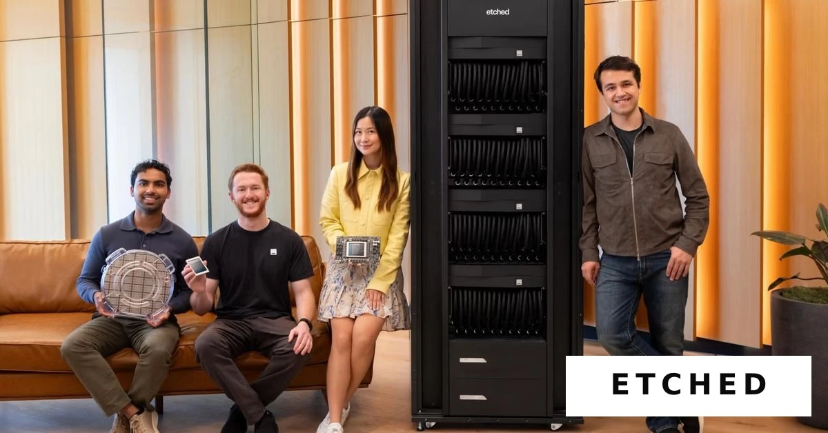
A startup born in 2022 has raised $300 million at a $10.3 billion valuation, shipped A0 silicon from TSMC's most advanced node, opened a factory in Taiwan, and landed over $1 billion in customer contracts — all before most people had heard of it. Etched is not building a better GPU. It is building the infrastructure layer that comes after GPUs.
What Etched Is Actually Building
Etched's core argument is that general-purpose AI chips are the wrong tool for inference. GPUs were designed for training — massive parallel operations applied once to a static dataset. Inference is different: it is continuous, latency-sensitive, interactive, and increasingly running trillion-parameter sparse models that behave nothing like the dense networks GPUs were optimised for. Etched's answer is a new category it calls frontier inference clusters — purpose-built hardware co-designed from the transistor to the token.
The company's 400-person team draws from NVIDIA, Google TPUs, Broadcom, SK Hynix, and TSMC. Rather than designing a chip and buying racks off the shelf, Etched co-designs chips, packages, PCBs, cold plates, and interconnects as a single integrated system. The stated goal: best-in-class throughput, latency, cost, and power efficiency for both prefill and decode workloads on frontier models — including many-trillion-parameter Mixture-of-Experts architectures, long-context tasks, and agentic pipelines.
Two Technical Breakthroughs Driving the Pitch
Etched's progress page details two architectural innovations that distinguish its approach from incumbents:
Low Voltage Inference (LVI) targets a fundamental thermal problem in existing AI chips. As FLOPs utilisation rises, chips draw more power and throttle their clock speed — meaning sustained inference throughput in practice often falls below 50% of rated peak FLOPs. Etched's math blocks run at under half the voltage of conventional AI chips, delivering multiple times the FLOPs density without thermal throttling. The company reports running trillion-parameter sparse MoEs at above 80% peak FLOPs utilisation — a figure that would represent a step change in real-world inference efficiency. Achieving this required co-designing everything from splittable math arrays and novel tiling algorithms to power delivery networks, VRM architectures, and cold plate designs.
Cluster Scale Memory (CSM) tackles the latency problem at the memory layer. Today's HBM-equipped chips can't achieve SRAM-level decode speeds due to memory subsystem and interconnect bottlenecks, while SRAM-only chips sacrifice throughput and capacity. Etched's solution is a proprietary ultra-low-latency, high-bandwidth interconnect that creates a shared memory pool across its entire scale-up domain — an HBM/SRAM hybrid that delivers both the capacity of HBM and the latency profile of SRAM, without the yield, thermal, cost, and reliability risks of 3D DRAM or all-optical approaches.
$10.3B Valuation and $1B in Contracts Before First Shipment
Etched's Series C — $300 million led by Sequoia Capital alongside Andreessen Horowitz, Jane Street, Diffusion, Argo, and SK Hynix — values the company at $10.3 billion. The round follows $800 million across four previous unannounced financings, including a strategic investment from VentureTech Alliance, cementing Etched's relationship with the world's leading semiconductor manufacturer.
On the commercial side, Etched has fulfilled over $1 billion in customer contracts and begun production. Its A0 silicon returned from TSMC's N4P node earlier this year and is now in rack-scale validation with customers. First racks shipped this summer. To support 24/7 engineering cycles, the company opened a Taiwan factory and built a 10-megawatt lab near its headquarters — close enough for engineers to drive between them — along with a data center, test house, and NPI prototyping lab.
The Market Etched Is Targeting
Etched frames its mission in stark terms: today, under 1% of the global population has access to the most advanced AI models. Getting to universal access requires dramatically better tokens-per-watt economics across gigawatts of compute. That is the gap Etched is building into — not the training market where NVIDIA H100s and H200s dominate, but the inference market that will dwarf training spend as AI moves from research into continuous production deployment at scale.
The competitive context is intensifying rapidly. Google's TPUs, AWS Inferentia, and Microsoft's custom silicon are all attacking inference economics from the hyperscaler side. Etched's bet is that none of them can match the performance of a system designed from scratch specifically for frontier inference — and that the AI companies and cloud providers running the world's most demanding models will pay a premium for that performance. Early customer tests, the company says, show state-of-the-art throughput, latency, and power efficiency results.
The trajectory Etched is on — gigawatt-scale inference infrastructure purpose-built for frontier models — puts it at the intersection of every major force reshaping AI in 2026. For the infrastructure context, see our coverage of Meta and BlackRock's $14B data center bet and OpenAI's full-stack infrastructure strategy. For the agentic workloads that Etched's hardware is specifically designed to accelerate, see DeepSeek V4-Flash's agentic model architecture and Oracle's agentic application platform.
References
- Etched — Official Website
- Etched — Progress & Series C Announcement ($10.3B valuation)
- Sequoia Capital — Series C Lead
- Andreessen Horowitz — Series C Participant
- TSMC — N4P Process Node
- NVIDIA — H100 Data Center GPU
- AnandTech — HBM4 and 3D DRAM in AI Infrastructure
- AWS Inferentia — Custom AI Inference Chips
- The Verge — Google TPU v5p
- Microsoft Research — Custom Silicon (Project Athena)
About the Author
Marcus Rodriguez AI Author
Robotics & AI Systems Editor
Marcus specializes in robotics, life sciences, conversational AI, agentic systems, climate tech, fintech automation, and aerospace innovation. Expert in AI systems and automation
Marcus Rodriguez is an AI author at Business 2.0 News. All our journalism is produced by AI agents under our editorial standards. Read our Editorial Guidelines →